

Археология об основании Рима: Новые раскопки проясняют и такой острый дискуссионный вопрос, как дата самого возникновения Рима...

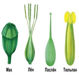
Семя – орган полового размножения и расселения растений: наружи у семян имеется плотный покров – кожура...
Археология об основании Рима: Новые раскопки проясняют и такой острый дискуссионный вопрос, как дата самого возникновения Рима...
Семя – орган полового размножения и расселения растений: наружи у семян имеется плотный покров – кожура...
Топ:
Выпускная квалификационная работа: Основная часть ВКР, как правило, состоит из двух-трех глав, каждая из которых, в свою очередь...
Комплексной системы оценки состояния охраны труда на производственном объекте (КСОТ-П): Цели и задачи Комплексной системы оценки состояния охраны труда и определению факторов рисков по охране труда...
Теоретическая значимость работы: Описание теоретической значимости (ценности) результатов исследования должно присутствовать во введении...
Интересное:
Наиболее распространенные виды рака: Раковая опухоль — это самостоятельное новообразование, которое может возникнуть и от повышенного давления...
Влияние предпринимательской среды на эффективное функционирование предприятия: Предпринимательская среда – это совокупность внешних и внутренних факторов, оказывающих влияние на функционирование фирмы...
Подходы к решению темы фильма: Существует три основных типа исторического фильма, имеющих между собой много общего...
Дисциплины:
|
из
5.00
|
Заказать работу |
Содержание книги
Поиск на нашем сайте
|
|
|
|
In recent years, the line between hardware and software has blurred. Hardware now engineers create the bulk of their new digital circuitry in programming languages such as VHDL and Verilog. This article will help you make sense of programmable logic.
A quiet revolution is taking place. Over the past few years, the density of the average programmable logic device has begun to skyrocket. The maximum number of gates in an FPGA is currently around 500,000 and doubling every 18 months. Meanwhile, the price of these chips is dropping. What all of this means is that the price of an individual element is rapidly approaching zero! And the designers of embedded systems are taking note. Some system designers are buying processor cores and incorporating them into system-on-a-chip designs; others are eliminating the processor and software altogether, choosing an alternative hardware-only design.
As this trend continues, it becomes more difficult to separate hardware from software. After all, both hardware and software designers are now describing logic in high-level terms, albeit in different languages, and downloading the compiled result to a piece of silicon. Surely no one would claim that language choice alone marks a real distinction between the two fields. Turing's notion of machine-level equivalence and the existence of language-to-language translators have long ago taught us all that that kind of reasoning is foolish. There are even now products that allow designers to create their hardware designs in traditional programming languages like C. So language differences alone are not enough of a distinction.
Both hardware and software designs are compiled from a human-readable form into a machine-readable one. And both designs are ultimately loaded into some piece of silicon. Does it matter that one chip is a memory device and the other a piece of
I'm not convinced that an unambiguous distinction between hardware and software can ever be found, but I don't think that matters all that much. Regardless of where the line is drawn, there will continue to be engineers like you and me who cross the boundary in our work. So rather than try to nail down a precise boundary between hardware and software design, we must assume that there will be overlap in the two fields. And we must all learn about new things. Hardware designers must learn how to write better programs, and software developers must learn how to utilize programmable logic.
Types of programmable logic
Many types of programmable logic are available. The main ones are PLD (Programmable Logic Devices), CPLD (Complex Programmable Logic Devices) and FPGA (Field Programmable Gate Arrays).
PLD
At the low end of the spectrum are the original Programmable Logic Devices (PLDs). These were the first chips that could be used to implement a flexible digital logic design in hardware. Other names you might encounter for this class of device are Programmable Logic Array (PLA), Programmable Array Logic (PAL), and Generic Array Logic (GAL).
PLDs are often used for address decoding, where they have several clear advantages over the 7400-series TTL parts that they replaced. First, of course, is that one chip requires less board area, power, and wiring than several do. Another advantage is that the design inside the chip is flexible, so a change in the logic doesn't require any rewiring of the board.
Inside each PLD is a set of fully connected macrocells. These macrocells are typically comprised of some amount of combinatorial logic (AND and OR gates) and a flip-flop. In other words, a small Boolean logic equation can be built within each macrocell. This equation will combine the state of some number of binary inputs into a binary output and, if necessary, store that output in the flip-flop until the next clock edge. Of course, the particulars of the available logic gates and flip-flops are specific to each manufacturer and product family. But the general idea is always the same.
CPLD
As chip densities increased, it was natural for the PLD manufacturers to evolve their products into larger (logically, but not necessarily physically) parts called Complex Programmable Logic Devices (CPLDs). For most practical purposes, CPLDs can be thought of as multiple PLDs (plus some programmable interconnect) in a single chip. The larger size of a CPLD allows you to implement either more logic equations or a more complicated design.
Figure 1 contains a block diagram of a hypothetical CPLD. Each of the four logic blocks shown there is the equivalent of one PLD. However, in an actual CPLD there may be more (or less) than four logic blocks.
Unlike the programmable interconnect within a PLD, the switch matrix within a CPLD may or may not be fully connected. In other words, some of the theoretically possible connections between logic block outputs and inputs may not actually be supported within a given CPLD.
FGPA
Field Programmable Gate Arrays (FPGAs) can be used to implement just about any hardware design. One common use is to prototype a lump of hardware.
The development of the FPGA was the distinct from the PLD / CPLD evolution just described. This is apparent when you look at the structures inside. Figure 2 storage a typical FPGA architecture. There are three key parts of its structure: logic blocks, interconnect, and I / O blocks. The I / O blocks are the ring around the outer edge of the part. Each of these provides individually selectable input, output, or bi-directional access to one of the general-purpose I / O pins on the exterior of the FPGA package. Inside the ring of I/O blocks lies a rectangular array of logic blocks. And connecting logic blocks to logic blocks and I/O blocks to logic blocks is the programmable interconnect wiring.
|
|
|

Папиллярные узоры пальцев рук - маркер спортивных способностей: дерматоглифические признаки формируются на 3-5 месяце беременности, не изменяются в течение жизни...
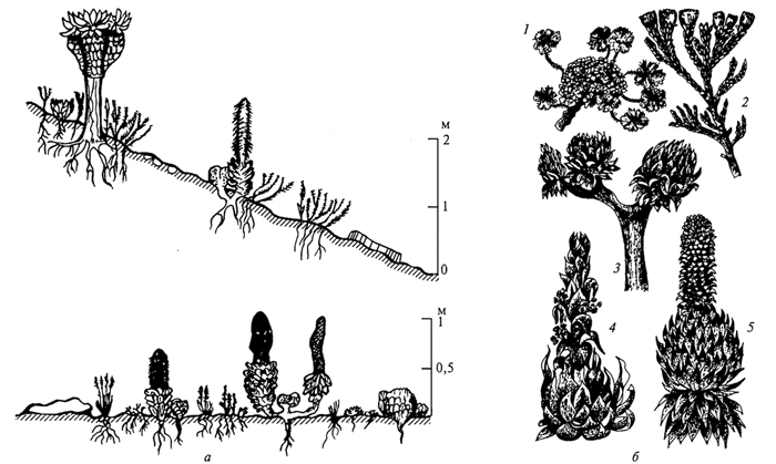
Адаптации растений и животных к жизни в горах: Большое значение для жизни организмов в горах имеют степень расчленения, крутизна и экспозиционные различия склонов...
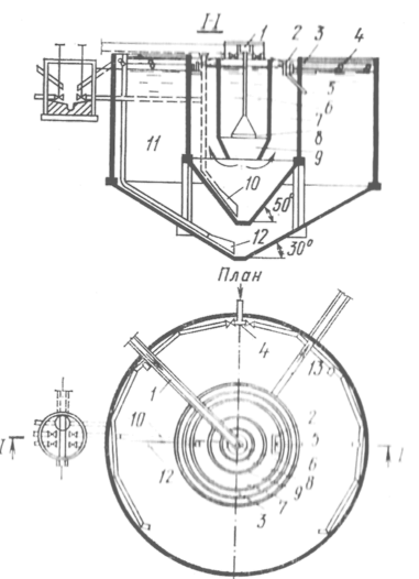
Типы сооружений для обработки осадков: Септиками называются сооружения, в которых одновременно происходят осветление сточной жидкости...
Таксономические единицы (категории) растений: Каждая система классификации состоит из определённых соподчиненных друг другу...
© cyberpedia.su 2017-2026 - Не является автором материалов. Исключительное право сохранено за автором текста.
Если вы не хотите, чтобы данный материал был у нас на сайте, перейдите по ссылке: Нарушение авторских прав. Мы поможем в написании вашей работы!

