
Своеобразие русской архитектуры: Основной материал – дерево – быстрота постройки, но недолговечность и необходимость деления...
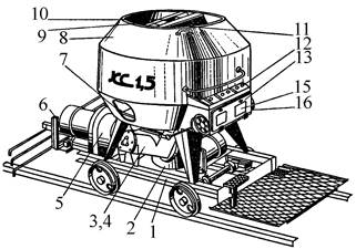
Кормораздатчик мобильный электрифицированный: схема и процесс работы устройства...
Своеобразие русской архитектуры: Основной материал – дерево – быстрота постройки, но недолговечность и необходимость деления...
Кормораздатчик мобильный электрифицированный: схема и процесс работы устройства...
Топ:
Оценка эффективности инструментов коммуникационной политики: Внешние коммуникации - обмен информацией между организацией и её внешней средой...
Когда производится ограждение поезда, остановившегося на перегоне: Во всех случаях немедленно должно быть ограждено место препятствия для движения поездов на смежном пути двухпутного...
Марксистская теория происхождения государства: По мнению Маркса и Энгельса, в основе развития общества, происходящих в нем изменений лежит...
Интересное:
Наиболее распространенные виды рака: Раковая опухоль — это самостоятельное новообразование, которое может возникнуть и от повышенного давления...
Подходы к решению темы фильма: Существует три основных типа исторического фильма, имеющих между собой много общего...
Влияние предпринимательской среды на эффективное функционирование предприятия: Предпринимательская среда – это совокупность внешних и внутренних факторов, оказывающих влияние на функционирование фирмы...
Дисциплины:
|
из
5.00
|
Заказать работу |
|
|
|
|
Exercise 1. Read and translate the text, using the words below.
There are three popular ways to describe the electronic structure of a crystal. The first starts from single atoms. An atom has discrete energy levels. When two atoms come close each energy level splits into an upper and a lower level, whereby they delocalize across the two atoms. With more atoms the number of levels increases and groups of levels form bands. Semiconductors contain many bands. If there is a large distance between the highest occupied state and the lowest unoccupied space, then a gap will likely remain between occupied and unoccupied bands even after band formation.
A second way starts with free electrons waves. When fading in an electrostatic potential due to the cores, due to Bragg reflection some waves are reflected and cannot penetrate the bulk, that is a band gap opens. In this description it is not clear, while the number of electrons fills up exactly all states below the gap.
A third description starts with two atoms. The split states form a covalent bond where two electrons with spin up and spin down are mostly in between the two atoms. Adding more atoms now is supposed not to lead to splitting, but to more bonds. This is the way silicon is typically drawn. The band gap is now formed by lifting one electron from the lower electron level into the upper level. This level is known to be anti-bonding, but bulk silicon has not been seen to lose atoms as easy as electrons are wandering through it. Also this model is most unsuitable to explain how in graded hetero-junction the band gap can vary smoothly.
When ionizing radiation strikes a semiconductor, it may excite an electron out of its energy level and consequently leave a hole. This process is known as electron–hole pair generation. Electron-hole pairs are constantly generated from thermal energy as well, in the absence of any external energy source.
Electron-hole pairs are also apt to recombine. Conservation of energy demands that these recombination events, in which an electron loses an amount of energy larger than the band gap, be accompanied by the emission of thermal energy (in the form of phonons) or radiation (in the form of photons).
In some states, the generation and recombination of electron–hole pairs are in equipoise. The number of electron-hole pairs in the steady state at a given temperature is determined by quantum statistical mechanics. The precise quantum mechanical mechanisms of generation and recombination are governed by conservation of energy and conservation of momentum.
As the probability that electrons and holes meet together is proportional to the product of their amounts, the product is in steady state nearly constant at a given temperature, providing that there is no significant electric field (which might move carriers of both types from neighbour regions containing more of them to meet together) or externally driven pair generation. The product is a function of the temperature, as the probability of getting enough thermal energy to produce a pair increases with temperature.
|
|
The probability of meeting is increased by carrier traps—impurities or dislocations which can trap an electron or hole and hold it until a pair is completed. Such carrier traps are sometimes purposely added to reduce the time needed to reach the steady state.
Words to be remembered.
to split – раскалывать; расщеплять
to fade – увядать; постепенно исчезать
core – сердцевина; внутренность; ядро; суть
to penetrate – проникать в; глубоко трогать; пронизывать
bulk – 1. масса 2. большая часть; основная масса 3. объём 4. внутренняя структура (например, полупроводника)
to spin up – свинчивать
bonds – узы; оковы
to wander – бродить; странствовать; блуждать
smoothly – гладко; плавно; спокойно
external – наружный, внешний
emission – выделение; испускание
equipoise – равновесие; противовес
precise – точный
trap – ловушка, уловитель
Exercise 2. Answer the following questions.
1. How many ways to describe the electronic structure of a crystal are there? Describe them.
2. What do semiconductors contain?
3. What model is the most unsuitable to explain how in graded hetero-junction the band gap can vary smoothly?
4. What is known as electron-hole pair generation?
5. What is apt to recombine?
6. What is determined by quantum statistical mechanics?
7. Is the product a function of the temperature or size?
8. What are impurities or dislocations which can trap an electron or hole and hold it until a pair is completed?
9. Why is such carrier traps sometimes purposely added?
10. What is electron-hole pairs constantly generated from?
Exercise 3. Find the proper Russian equivalents to the given English terms.
| 1. steady state | 1. единичные атомы |
| 2. popular ways | 2. тепловая энергия |
| 3. electronic structure | 3. уровень энергии |
| 4. unoccupied space | 4. устойчивое состояние |
| 5. single atoms | 5. электронная структура |
| 6. thermal energy | 6. соседние области |
| 7. energy source | 7. популярные способы |
| 8. conservation of energy | 8. незанятое пространство |
| 9. neighbour regions | 9. источник энергии |
| 10. energy level | 10. сохранение энергии |
Exercise 4. Translate the following sentences from Russian into English.
1. Существуют три известных способа описать электронную структуру кристалла. 2. У атома имеются прерывистые (дискретные) уровни энергии. 3. С увеличением атомов количество уровней возрастает, и группы уровней формируют зоны. 4. Третье описание касается двух атомов. 5. Сохранение энергии требует, чтобы эти события сопровождались испусканием термальной энергии или радиации. 6. Продукт является функцией температуры, как вероятности получить достаточно термальной энергии. 7. Такие ловушки иногда специально добавляются для того, чтобы снизить время, необходимое для достижения устойчивого состояния.
|
|
Exercise 5. Match the two parts of the sentence
1. There are three popular ways to describe …
a) the free electrons waves
b) the electronic structure of a crystal
c) the band formation
2. Semiconductors contain …
a) many bands
b) many bonds
c) many bandages
3. Adding more atoms now is supposed not to lead to splitting, …
a) but to more bonds
b) but to more bands
c) but to less bonds
4. The band gap is now formed by lifting one electron from …
a) the upper electron level into the lower level
b) the lower electron level into the upper level
c) the discrete energy level
5. Electron-hole pairs are constantly …
a) generated from water energy
b) generated from lightning energy
c) generated from thermal energy
6. The number of electron-hole pairs in the steady state at a given temperature …
a) is determined by quantum statistical mechanics
b) is determined by quantum statistical engineering
c) is determined by conservation of energy
7. The product is a function of the temperature, as the probability of getting enough thermal energy to produce a pair increases …
a) with time
b) with size
c) with temperature
8. Such carrier traps are sometimes purposely added to reduce …
a) the size needed to reach the steady state
b) the time needed to reach the steady state
c) the temperature needed to reach the steady state
Exercise 6. Topics for discussion:
1. Electronic structure
2. Carrier generation
3. Recombination
4. Carrier traps
CHAPTER 9. PREPARATION OF SEMICONDUCTOR MATERIALS (ПОДГОТОВКА ПОЛУПРОВОДНИКОВЫХ МАТЕРИАЛОВ)
Exercise 1. Read and translate the text, using the words below.
Semiconductors materials are materials which are insulators at absolute zero temperature but which conduct electricity at room temperature. The defining property of a semiconductor material is that it can be doped with impurities that alter its electronic properties in a controllable way.
Because of their application in devices like transistors (and therefore computers) and lasers, the search for new semiconductor materials and the improvement of existing materials is an important field of study in materials science.
Most commonly used semiconductor materials are crystalline inorganic solids. These materials are classified according to the periodic table groups of their constituent atoms.
Different Semiconductor materials differ in their properties. Thus, in comparison with silicon, Compound semiconductors have both advantages and disadvantages. For example, gallium arsenide has six times higher electron mobility than silicon, which allows faster operation; wider band gap, which allows operation of power devices at higher temperatures, and gives lower thermal noise to low power devices at room temperature; its direct band gap gives it more favorable optoelectronic properties than the indirect band gap of silicon; it can be alloyed to ternary and quaternary compositions, with adjustable band gap width, allowing light emission at chosen wavelengths, and allowing e.g. matching to wavelengths with lowest losses in optical fibers.
Semiconductors with predictable, reliable electronic properties are necessary for mass production. The level of chemical purity needed is extremely high because the presence of impurities even in very small proportions can have large effects on the properties of the material. A high degree of crystalline perfection is also required, since faults in crystal structure (such as dislocations, twins, and stacking faults) interfere with the semiconducting properties of the material. Crystalline faults are a major cause of defective semiconductor devices. The larger the crystal, the more difficult it is to achieve the necessary perfection.
|
|
Because of the required level of chemical purity and the perfection of the crystal structure which are needed to make semiconductor devices, special methods have been developed to produce the initial semiconductor material. A technique for achieving high purity includes growing the crystal using the Czochralski process. An additional step that can be used to further increase purity is known as zone refining. In zone refining, part of a solid crystal is melted. The impurities tend to concentrate in the melted region, while the desired material recrystalizes leaving the solid material more pure and with fewer crystalline faults.
In manufacturing semiconductor devices involving heterojunctions between different semiconductor materials, the lattice constant, which is the length of the repeating element of the crystal structure, is important for determining the compatibility of materials.
Words to be remembered.
gallium arsenide – арсенид галлия
alloy – примесь; сплав
width – ширина; широта
fault – недостаток; дефект
twin – 1. двойник 2. пара Гото
stacking fault – дефект упаковки
perfection – совершенство; высшая степень
zone refining – зонная очистка
to melt – таять; плавить(ся)
compatibility – совместимость
Exercise 2. Answer the following questions.
1. At what temperature do semiconductor materials conduct electricity?
2. What is the defining property of a semiconductor material?
3. In what devices do semiconductor materials find their application?
4. What are the most commonly used semiconductor materials? How are they classified?
5. How do semiconductor materials differ?
6. What semiconductors are necessary for mass production?
7. What is a major cause of defective semiconductor devices?
8. What does a technique for achieving high purity include?
9. What is zone refining?
10. What is important for determining the compatibility of materials?
Exercise 3. Read the phrases, remember them and make up your own sentences with the new word expressions.
Controllable way, periodic table, electron mobility, light emission, optical fibers, mass production, required level, extremely high, semiconducting properties, melted region.
Exercise 4. Translate the sentences from Russian into English.
1. Полупроводниковые материалы проводят электричество при комнатной температуре. 2. Из-за того что полупроводники применяются в таких устройствах как транзисторы и лазеры, необходимо искать новые полупроводниковые материалы и улучшать существующие. 3. Эти материалы классифицируются по группам периодической таблицы. 4. Полупроводниковые материалы различаются по своим свойствам. 5. Полупроводники с предсказуемыми, надёжными электронными свойствами необходимы для массового производства. 6. Кристаллические дефекты являются главной причиной бракованных полупроводниковых устройств. 7. Электронная мобильность арсенида галлия в шесть раз выше, чем у кремния.
|
|
Exercise 5. Complete the following sentences.
1. … are necessary for mass production. 2. Crystalline faults are a major cause of … 3. … special methods have been developed to produce the initial semiconductor material. 4. … part of a solid crystal is melted. 5. The defining property of a semiconductor material is that … 6. Most commonly used semiconductor materials are … 7. … have both advantages and disadvantages. 8. Because of their application in devices like transistors and lasers … 9. The impurities tend to concentrate in the melted region, while … 10. A technique for achieving high purity includes …
Exercise 6. Substitute the Russian words for the English ones.
1. Semiconductor materials are materials which are изоляторы at absolute zero temperature.
a) conductors
b) insulators
c) generators
2. Semiconductor materials differ in their свойства.
a) particles
b) substances
c) properties
3. Присутствие of impurities can have large effects on the properties of the material.
a) the presence
b) the present
c) the pleasant
4. Crystalline дефекты are a major cause of defective semiconductor devices.
a) defects
b) faults
c) effects
5. The larger the crystal, the more difficult it is to achieve the necessary совершенство.
a) perfection
b) perfect
c) preference
6. An additional step that can be used to further увеличение purity is known as zone refining.
a) decrease
b) shorten
c) increase
Exercise 7. Read an additional text and tell what you have understood from it.
Symbols and Abbreviations
The symbols used for quantities in electrical engineering can be confusing, since the symbol for a quantity may be different from the symbol for the units in which it is measured. We list the common symbols here, even though some of the concepts have not yet been defined.
Electrical charge is typically denoted Q, measured in coulombs, abbreviated C. However, electrical engineers rarely refer to charge, and the letter C is usually used to denote capacitance.
Example:  is the theoretical formula for a capacitor's behavior—the charge is the product of the capacitance times the voltage.
Current is typically denoted I, measured in amperes, abbreviated A.
An ampere is, among other things, a coulomb per second.
Example:  Ohm's law; voltage equals current times resistance.
Example: "  " "The current is 28 milliamperes."
Voltage is typically denoted V (or sometimes E), and measured in volts, abbreviated V. The use of " E " stands for "emf" (electro-motive force.)
A volt is, among other things, a joule per coulomb.
Example: "  " "The voltage is 28 millivolts."
Resistance is typically denoted R, measured in ohms, abbreviated with the capital Greek omega: Ω.
An ohm is, among other things, a volt per ampere.
Example: "  " "The resistance is 2.7 kilohms."
It is sometimes useful to speak of the reciprocal of resistance. This is called conductance, and is typically denoted G, traditionally measured in "mhos" ("mho" is "ohm" spelled backwards), abbreviated with an upside-down omega:  . A less flippant term than "mho" has been adopted: the siemens, abbreviated S.
A mho/siemens is, among other things, an ampere per volt.
Example:  Ohm's law rewritten in terms of conductance.
Example: "  " "The conductance is 65 milliohms."
Example: "  " "The conductance is 65 millisiemens."
Capacitance is typically denoted C, measured in farads, abbreviated f.
A farad is, among other things, a second per ohm, or a coulomb per volt.
Example:  The time constant is the resistance times the capacitance.
Example: "  " "The capacitance is 75 picofarads."
Inductance is typically denoted L, measured in henries, abbreviated h.
A henry is, among other things, an ohm-second.
Example:  is the formula for the frequency of a resonant circuit.
Example: "  " "The inductance is 120 nanohenries."
Power is typically denoted P, measured in watts, abbreviated W.
A watt is, among other things, a joule per second, or a volt-ampere.
Example:  The power is the voltage times the current.
Example: "  " "The power is 75 watts."
The frequency of an oscillation or signal is typically denoted f, measured in hertz, abbreviated Hz.
A hertz is really just a reciprocal second. In fact, the unit of frequency used to be just "cycles per second" or simply "cycles".
Example: "  " "102.5 megacycles on the FM dial" (old way.)
|
|
Example: "  " "102.5 megahertz on the FM dial" (new way.)
UNIT III
|
|
|
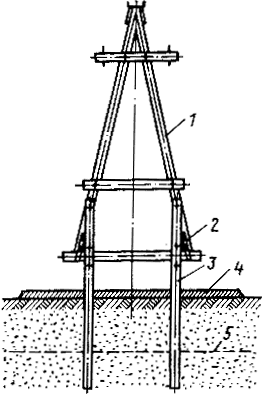
Особенности сооружения опор в сложных условиях: Сооружение ВЛ в районах с суровыми климатическими и тяжелыми геологическими условиями...
Своеобразие русской архитектуры: Основной материал – дерево – быстрота постройки, но недолговечность и необходимость деления...
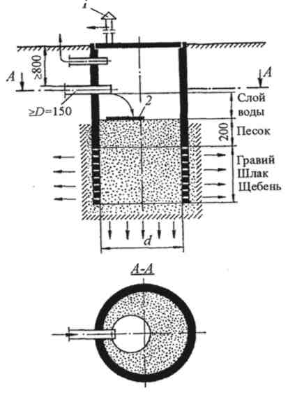
Индивидуальные очистные сооружения: К классу индивидуальных очистных сооружений относят сооружения, пропускная способность которых...
История развития пистолетов-пулеметов: Предпосылкой для возникновения пистолетов-пулеметов послужила давняя тенденция тяготения винтовок...
© cyberpedia.su 2017-2024 - Не является автором материалов. Исключительное право сохранено за автором текста.
Если вы не хотите, чтобы данный материал был у нас на сайте, перейдите по ссылке: Нарушение авторских прав. Мы поможем в написании вашей работы!