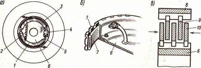
Автоматическое растормаживание колес: Тормозные устройства колес предназначены для уменьшения длины пробега и улучшения маневрирования ВС при...
Кормораздатчик мобильный электрифицированный: схема и процесс работы устройства...
Автоматическое растормаживание колес: Тормозные устройства колес предназначены для уменьшения длины пробега и улучшения маневрирования ВС при...
Кормораздатчик мобильный электрифицированный: схема и процесс работы устройства...
Топ:
Особенности труда и отдыха в условиях низких температур: К работам при низких температурах на открытом воздухе и в не отапливаемых помещениях допускаются лица не моложе 18 лет, прошедшие...
Теоретическая значимость работы: Описание теоретической значимости (ценности) результатов исследования должно присутствовать во введении...
Генеалогическое древо Султанов Османской империи: Османские правители, вначале, будучи еще бейлербеями Анатолии, женились на дочерях византийских императоров...
Интересное:
Наиболее распространенные виды рака: Раковая опухоль — это самостоятельное новообразование, которое может возникнуть и от повышенного давления...
Лечение прогрессирующих форм рака: Одним из наиболее важных достижений экспериментальной химиотерапии опухолей, начатой в 60-х и реализованной в 70-х годах, является...
Отражение на счетах бухгалтерского учета процесса приобретения: Процесс заготовления представляет систему экономических событий, включающих приобретение организацией у поставщиков сырья...
Дисциплины:
|
из
5.00
|
Заказать работу |
Depending on the kind of impurity, a doped region of semiconductor can have more electrons or holes, and is named N-type or P-type semiconductor material, respectively. Junctions between regions of N- and P-type semiconductors create electric fields, which cause electrons and holes to be available to move away from them, and this effect is critical to semiconductor device operation. Also, a density difference in the amount of impurities produces a small electric field in the region which is used to accelerate non-equilibrium electrons or holes.
In most semiconductors, when electrons lose enough energy to fall from the conduction band to the valence band (the energy levels above and below the band gap), they often emit light, a quantum of energy in the visible electromagnetic spectrum. This photoemission process underlies the light-emitting diode (LED) and the semiconductor laser, both of which are very important commercially. Conversely, semiconductor absorption of light in photo detectors excites electrons to move from the valence band to the higher energy conduction band, thus facilitating detection of light and vary with its intensity. This is useful for fiber optic communications, and providing the basis for energy from solar cells.
In classic crystalline semiconductors, the electrons can have energies only within certain bands (i.e. ranges of levels of energy). Energetically, these bands are located between the energy of the ground state, corresponding to electrons tightly bound to the atomic nuclei of the material, and the free electron energy. The latter is the energy required for an electron to escape entirely from the material. The energy bands each correspond to a large number of discrete quantum states of the electrons, and most of the states with low energy (closer to the nucleus) are full, up to a particular band called the valence band. Semiconductors and insulators are distinguished from metals because the valence band in the semiconductor materials is nearly filled under usual operating conditions, thus causing more electrons to be available in the "conduction band," the band immediately above the valence band.
The ease with which electrons in a semiconductor can be excited from the valence band to the conduction band depends on the band gap between the bands. The size of this energy band gap serves as an arbitrary dividing line between semiconductors and insulators.
With covalent bonds, an electron moves by hopping to a neighboring bond. The Pauli Exclusion Principle requires the electron to be lifted into the higher anti-bonding state of that bond. For delocalized states, for example in one dimension – that is in a nanowire, for every energy there is a state with electrons flowing in one direction and another state with the electrons flowing in the other. For a net current to flow, more states for one direction than for the other direction must be occupied. For this to occur, energy is required, as in the semiconductor the next higher states lay above the band gap. Often this is stated as: full bands do not contribute to the electrical conductivity. However, as the temperature of a semiconductor rises above absolute zero, there is more energy in the semiconductor to spend on lattice vibration and — more importantly for us — on lifting some electrons into an energy states of the conduction band. The current-carrying electrons in the conduction band are known as "free electrons", although they are often simply called "electrons" if context allows this usage to be clear.
Electrons excited to the conduction band also leave behind electron holes, or unoccupied states in the valence band. Both the conduction band electrons and the valence band holes contribute to electrical conductivity. The holes themselves don't actually move, but a neighboring electron can move to fill the hole, leaving a hole at the place it has just come from, and in this way the holes appear to move, and the holes behave as if they were actual positively charged particles.
One covalent bond between neighboring atoms in the solid is ten times stronger than the binding of the single electron to the atom, so freeing the electron does not imply destruction of the crystal structure.
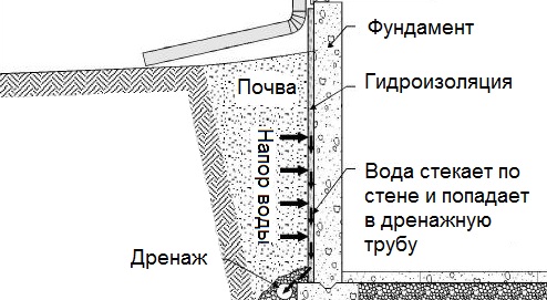
Общие условия выбора системы дренажа: Система дренажа выбирается в зависимости от характера защищаемого...
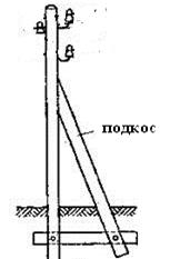
Опора деревянной одностоечной и способы укрепление угловых опор: Опоры ВЛ - конструкции, предназначенные для поддерживания проводов на необходимой высоте над землей, водой...
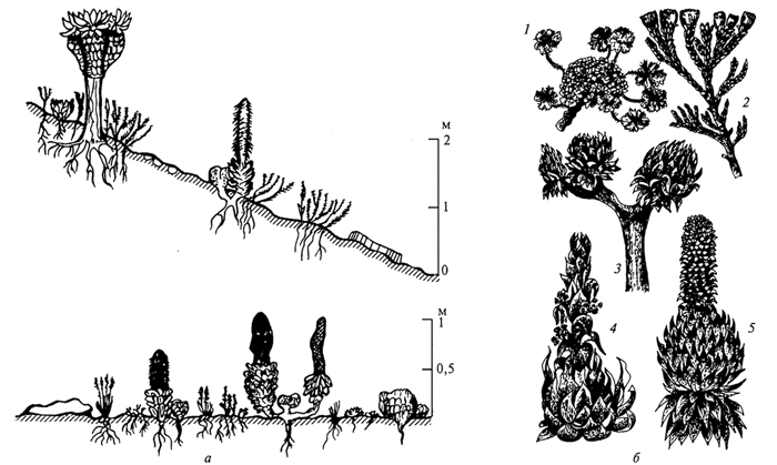
Адаптации растений и животных к жизни в горах: Большое значение для жизни организмов в горах имеют степень расчленения, крутизна и экспозиционные различия склонов...
Типы сооружений для обработки осадков: Септиками называются сооружения, в которых одновременно происходят осветление сточной жидкости...
© cyberpedia.su 2017-2024 - Не является автором материалов. Исключительное право сохранено за автором текста.
Если вы не хотите, чтобы данный материал был у нас на сайте, перейдите по ссылке: Нарушение авторских прав. Мы поможем в написании вашей работы!